
The challenge
To stay competitive in today’s semiconductor industry, innovation is key. Typical R&D spend amounts up to 15% of the total product revenue. Hardware designs must be flawless; chip production has no “undo button”. The challenge for R&D is to design and release new products as quickly as possible, at lowest cost and minimum failure rate.
The R&D Design Flow Optimizer explained
The R&D design process from logical to physical design and then to tape-out typically runs thousands of design simulations using EDA (Electronic Design Automation) tools from vendors like Cadence and Spectre.
Typically, over 50 concurrent R&D projects are competing internally for limited pools of high-cost EDA licenses and on-premise compute clusters that could support the entire IT needs of a medium-sized enterprise.
The question
Fortunately, the flexibility of the cloud enables R&D to scale up instantly and reduce simulation times considerably. But this comes at a cost. While R&D projects are using hundreds of millions of CPU hours on design simulations, cloud spend adds up to millions of dollars monthly.
R&D faces a delicate balance between time to market, cost, and failure rate.
Can we optimize this? That is what we asked ourselves, with our large customer base in SemiCon and our experience in R&D design flows, EDA tools, cloud, optimization algorithms, and recently GenAI. Yes, we can!
The solution
For one of our customers, we combined our existing knowledge on optimization algorithms, GenAI prompting, and cloud cost control - to build an R&D design flow optimizer. This optimizer provides a slider for R&D teams and managers to run design simulations optimally, either at the lowest cost or the fastest time to market.

How does it work?
The optimizer follows a strategy to optimize R&D design flows in 4 areas:
- Best fit R&D demand characteristics: R&D projects and EDA simulation types
- Select best fit cost model per R&D project demand
- Select best fit time slot for R&D project priorities
- Right-size cloud resources to match the EDA simulation types
Three-step approach
We use a three-step approach to embed the optimizer in R&D’s daily way of working.
Step 1 is to give the R&D project lead insights into his current project demand and a logical choice between speed and cost of design simulations and tape-outs. In other words, start with a conversation on what is most important for your product release:
- Do I need to run my simulations as fast as possible to meet the release deadline? Get priority above other R&D projects for my tape-out?
- Or can I save money by waiting for on-prem resources to become available, or make use of cheaper cloud reserved or spot instances?
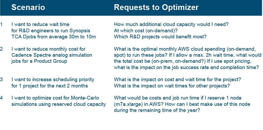
Typical R&D user questions that the optimizer answers are:
Step 2 is to merge both on-prem and cloud environment to a seamless R&D design platform, so that the R&D teams have the flexibility to choose where EDA workloads (e.g., design simulations, tape-outs) will run: Using on-premise compute when available, and cloud compute when needed.
Step 3 is to run the optimization algorithms (what-if scenarios) based on the choice of the R&D project leads and the usage data of the R&D platform, so that actual simulations run at the lowest cost or fastest time possible.
The optimizer uses input from the user (project constraints such as maximum allowed wait time, maximum cost), actual and historical EDA simulations queued (overview of simulations from other users/projects in the LSF scheduler queues), resource utilization (on-prem and cloud utilization of CPU, memory, licenses) and actual pricing of three cloud cost models (spot, on-demand, reserved).
The optimizer shows you how to schedule your simulations optimally using your resource reservations, budget, and remaining simulation time before the next product release. After R&D agrees, the scheduler configuration will automatically adjust.
The value
So, what is the value of the R&D design flow optimizer? Cost savings up to 40%, reduction of R&D engineering wait times to near-zero, increase of resource utilization up to 80%. And most of all: R&D to have insight and control in cost and time to market of the next product release.